
The sorting step is required for LTGEN which will create bond fingers.

|
Package designers generally get information about the die
in a netlist format. This data needs to be entered into AutoCAD if you wish to create
bond wire diagrams or if you wish to design a BGA package for the chip.
Artwork has developed a simple yet easy-to-use program called Die Import that reads a die netlist and automatically draws the chip in AutoCAD. |
Features
|
|
|
We added features requested by our clients: Automatic centering if
the original netlist coordinates are not centered around 0,0. Rotation: you can insert
the chip at 0,90,180, or 270 degrees.
Counting PAD Types |
||
|
|
At left you can see the results of importing a rectangular die
with 288 pads. The entire process takes about 5 seconds to create the
pads and another 20-30 seconds to sort them by top/bottom/left and
right. The sorting step is required for LTGEN which will create bond fingers. |
|
User Interface
|
|
|
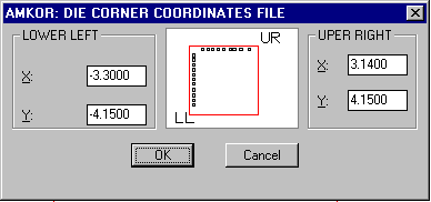
Main Menu - collects
the required information to draw and place the die. The user specifies the die netlist and a keyword file for power and ground nets. If the die edge is not symmetric with respect to the pads then the user should also enter the corner coordinates; otherwise entering the die width and height is sufficient. |

|
|
PAD Report
|
|

|
Die Report - shows the number of I/O, Power, Ground and No Connect PADS on each side of the die. This information is useful to BGA designers who need to know how many bond fingers to use on each side of the package. |
|
Additional Program Details |
|||
| Program Flow | Netlist Format | Keyword File for Power, Ground and No Connect | |