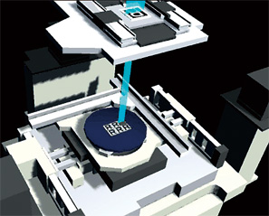
Reticle Input Data

IC's are made using a reticle that is stepped across the surface of the wafer. The reticle is a mask that is 4X or 5X the actual size of the device features. To increase throughput, the reticle will have several devices arrayed on it so that the reticle's step size is some multiple of the step size of the actual device.
The information that the foundry provides the packaging engineer is generally in terms of the reticle size, step, offset and number of die in the reticle.
The mask designer for the flipchip does not really care about a reticle -- all he cares about are getting the die in the right place. The GDS-SR automation software can take reticle input directly. It steps the reticle and "removes" any die that fall outside the margin or wafer extents. This avoids potential errors by manually dividing reticle dimensions into die dimensions.