Wafer Level Mask Tools Page Header


Introduction

Steve DiBartolomeo
Applications Manager
Steve DiBartolomeo

More and more chips are packaged using flip chip or wafer level packaging technologies. These packages require wafer sized masks to build up and etch geometries directly onto the wafer supplied by the chip foundry. Producing these mask sets requires that one properly layout and align all data with the underlying chip positions and pad openings.
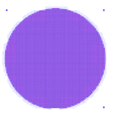
image of wafer mask


There are two distinct design jobs - the first is to create the individual chip's redistribution layers. This usually consists of a VIA1 layer, an RDL layer, a second via layer, a UBM (under bump metal) layer and a solder mask layer. These designs are usually done using a package layout software such as Cadence APD though for low pin count designs one can even use a mechanical software such as AutoCAD.

unit cell design

The second design job is to array this "circuit" so that the pattern of circuits (along with any alignment or test devices) matches exactly the positions of the chips on the wafer.

wafer_layout

We are describing tools for this second part of the design effort.


Contents

Wafer Diameter/Margin/Notch

Step & Repeat Parameters

Dealing with Reticle Data

Knock Out Die to Reveal Underlying Features

Drop in Alignment and Test Die

Leaving Sacrificial Die for Clipping

Creating a SINF output File


Clip Array to a Round Circle

Removing Slivers during Clip

Merging Data from External Files

Final Mask Set Output

Viewing and Checking Results

Auto Documentation of Unit Cell

Auto Documentation of Wafer Layout

Video - Multi Product Wafer in 10 minutes