Package designers would like to be able to import a package bond diagram done in AutoCAD into Cadence APD/SIP for a variety of reasons -- one of the most interesting is to use APD as an interface to simulation tools such as those offered by Sigrity, Optimal and Ansoft. [Ed note: you can tell when this was written because all three of these simulation companies have since been acquired]
The import must be intelligent -- that is, one must construct a valid APD database with symbols, nets, conductors, die and wires. Therefore the basic DXF import offered by APD is completely unsuitable for this purpose.
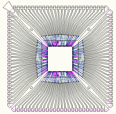
We will take a real life example (seen at right) and describe the steps required to import the data contained in the drawing intelligently into APD.

Leadframe drawn in AutoCAD with Die and Wires
APD/SIP runs on top of a very rigorous database which insures the integrity of a design. One cannot willy-nilly bring in external data and expect it to be understood by SIP. There are very clear requirements that must be met.
A layer crossection must be defined. This is necessary not only for the padstack definitions but needed when placing the symbols.
Symbols must be created - for a package at least two symbols are needed - a die symbol and an IO (substrate) symbol. A symbol consists of a set of pads (generally defined by a pad stack) where each pad has a coordinate and a label. A package outline is normally part of the symbol. For stacked die and multi-chip modules there may be more than one die symbol.
Padstacks padstacks must be created for the symbols and any vias. This might be a simple rectangular pad for the die pads and a round or rectangular pad for the leadframe (even though it does not actually have such pads on it!)
A Netlist must be created. The netlist defines the connections between the pins on the symbols.
Conductor data must first be "conditioned" to make it acceptable for import into APD. Conductors can be either shapes or traces.
Vias must be identified and associated with layers in the crossection and with a padstack.
Wires need to be identified and associated with either die pads or a conductor.
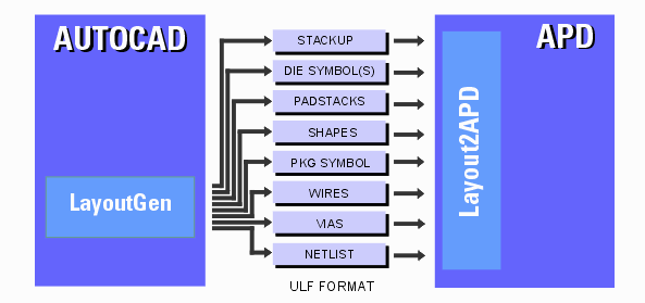
Identifying and organizing the AutoCAD data is accomplished interactively inside of AutoCAD using the module called LayoutGen. LayoutGen writes the intelligent data to an ASCII file format we developed called ULF (universal layout format). Since the ULF contains everything one needs to know about a design, we should be able to write translators from ULF to a variety of other formats in the future.

Once the LayoutGen work is complete and one has a ULF (universal layout format) file, the second step is to import that data into APD in order to create a valid database. When importing data into APD a specific flow must be adhered to. For example, one has to define the crossection first - otherwise the pad stack definitions will make no sense. A netlist must be imported prior to placement of the symbols. Wires can only be created after the die has been placed and the target conductor has been placed.
All these tasks are done by a SKILL module called Layout2APD
Lead frame packages must have a lead or wing that connects from the plane of the package down to the PCB. In many cases this is in the shape of a "gull wing" though there are packages with "J" shaped leads and even leadless packages. However these complicated shapes cannot be passed to APD or other layout tools because they assume conductors are thin planes.
In order to model the "gull wing" that connects the conductor plane of the package to the top of the PCB we will approximate it by using a long via that has the same crossection as the gull wing.
