The Players
The following companies seem to be the "players" in the new world of direct write lithography for PCBs and advanced IC packages. The data below is collected from their WEB pages.
Aiscent Technologies (China)
Aiscent Technologies LDI features a proprietary data processing system that "can process image files on-the-fly without waiting time to ensure fast and accuracy scanning even for a large exposure area."
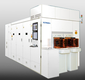
They have a machine (DW-3000) designed for direct writing onto finished wafers (primarily for the packaging market where packages are built directly onto wafers ...) It has 3 um resolution, up to 300 mm wafer, can write both the die and the ID (dynamic text) and so on. 64 wafers per hour means less than 1 minute per 300 x 300 area.
Update Dec 2017 - a recent review of their web site shows a new machine - the DW-6000 designed for panel level packages. This supports die-by-die alignment and supports panels up to 620 x 650 mm. They claim to support up to 70 panels per hour at 5 um L/S and on a 500 x 500 mm panel.
ADTEC Technology supplies direct imaging exposure systems with world-leading balance of quality, speed, and stability. ADTEC Technology acquired the division of Fuji Film with its Inprex LDI. They also acquired Via Mechanics group with their line of direct exposure systems DE-2 and DE-8.
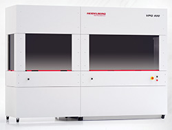
Their new VPG line - small area (200 and 400) uses a high power DPSS laser and supports substrates of up to 8" and 16" respectively. the VPG 1100 supports large panels ranging in size from 800 x 800 mm up to 1400 x 1400 mm.
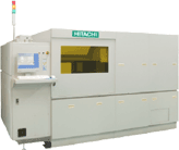
Family of direct digital exposure equipment ... DE-6UH Series
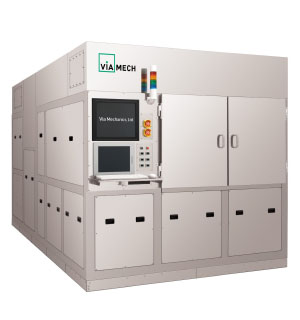
Update Dec 2017 - the DE-8WH, a new machine for FOWLP was announced in July 2017. It can expose 2 um L/S with plus/minus 1 um overlay. The machine can process 620 x 620 um panels or 300 mm wafers.
Japan Science Engineering Co. Ltd. (DNK)
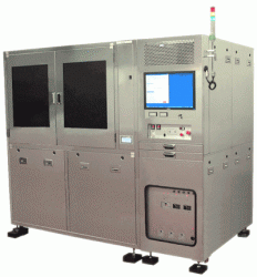
Direct Write machine developed by Index Technologies
| MX-101 | MX-201 | MX-1301E | MX-1702 | |
| Line Width (min) | 5 um | 5 um | 3 um | 10 um |
| Image Resolution | 0.5 um | 0.5 um | 0.25 um | 1.0 um |
| Image Area | 100 x 100 mm | 200 x 200 mm | 300 x 300 mm | 550 x 650 mm |
| Laser Wavelength | 375 nm | 405 nm | 405 nm | 405 nm |
| Exposure Scan Speed | 43.9 mm/sec | 43.9 mm/sec | 22.5 mm/sec | 92.2 mm/sec |
| Number of Heads | 1 | 1 | 1 | 7 |
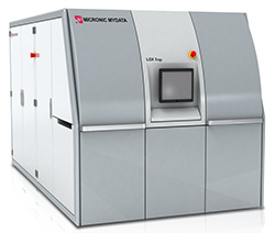
LDI 5s Series: UV direct writer (gray-scale approach) distortion correction. Uses 355 nm diode source and supports panels up to 510 x 515 mm. Twin stages - alignment and focus mapping on one while writing on the other.
Update Dec 2017 - Mycronic stopped development of their LDI efforts sometime in 2014 per their annual report.
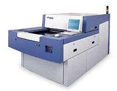
Paragon Ultra Family for PCBs and packages ... Orbotech was acquired by KLA Tencor.
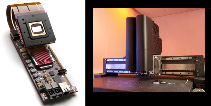
This Norweigan company sells a lithography system but main focus seems to be the light engines (DMD assembly, driver electronics) Texas Instruments design partner.
