Using Qckvu3 to Identify Faults
After a chip has been produced (generally for the first pass) and the wafer is sent to test, some faults are detected. There are various methods of finding faults - electrical testing can identify which pin/gate is not at the expected electrical level and thermal imaging/scanning can detect "hotspots" literally a small glowing spot caused by high current.
What causes such faults?
Aside from an error in the circuit design, faults can be caused by physical connectivity problems such as shorts or opens. Life is made difficult for the yield engineer who is searching for such a short/open because it may not be located right at the hotspot -- it may happen some distance away.
Finding the Fault
The fault will generally be found on a conductor that is part of the physical net that the hotspot identifies. So a yield engineer will want to trace back from the hot spot through the various nets to find the fault.
To narrow his search for shorts, the yield engineer would like to be able to pick a net, see all elements of the net and also have highlighted all proximate nets that need to be investigated. Because the net traverses many layers he may also wish to examine the proximate nets layer by layer.
Qckvu's NetTrace
Qckvu's NetTrace is an add-on module to the basic Qckvu that helps the yield engineer to find faults. It includes the following functionality:
-
Stackup Configuration
The user defines the metal and via layers that are to be traced through to determine connectivity.
Net TracingA high speed net tracer quickly highlights a net based on a "seed" or starting point.
Driver IdentificationIt is often useful when viewing a highlighted net, to identify where the "driver" or output devices are located on the net. This is accomplished by checking for a user defined combination of layers. Where multiple driver vias are closely spaced, a single driver box is created by combining the extents of these vias.
HotSpot Seed Point CreationA hot spot detected during thermal analysis is relatively large relative to a chips line width. Therefore it is likely that it cover multiple nets. This function returns all the nets located under a hot spots footprint.
Proximity Net HighlightingOnce a given net is to be examined the user can highlight any net which comes close to the net under consideration. This is quite helpful in searching for shorts between nets.
Branch Point ComputationIf two faults are located over the same net it is likely that the source of the fault lies somewhere on a branch of the net that lies between the two fault points. This function identifies the path between the two faults and ignores parts of the net that are not on the branch.
The Test File
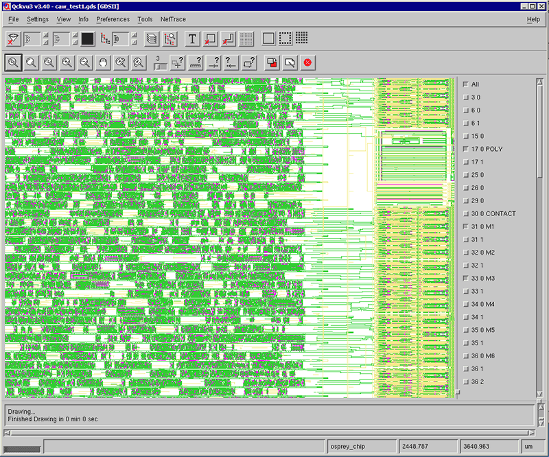
We will use a test file, caw_test1.gds, to illustrate the functionality of NetTrace and to define how the various functions work. This is a reasonably sized file (1.4GB) with seven layers of metal. We will focus on the overall region defined by:
LL = 2440, 3550 um to UR = 2620, 3690 um

Layer Stackup
While this design has many layers (and datatypes) the ones we are concerned with are:
Layer:Datatype   Physical Description
   17:0                 POLY
   30:0                 CONTACT
   31:0                 M1
   32:0                 M2
   33:0                 M3
   34:0                 M4
   35:0                 M5
   36:0                 M6
   37:0                 M7
   51:0                 VIA12
   52:0                 VIA23
   53:0                 VIA34
   54:0                 VIA45
   55:0                 VIA56
   56:0                 VIA67
