
To make a general purpose translator from 2D EDA into 3D MCAD one needs to use a format that is well supported by the major MCAD and simulation tools. The STEP specification has achieved significant adoption among almost all MCAD tools and it is this database we have selected as our connection to MCAD. [Ed Note: since the release of this product Artwork has addded support for the parasolid format which works much better with SOLIDWORKS than STEP does.]
Artwork has developed a 3Di to STEP translator that reads our 3Di format and creates STEP AP 203 or AP 214 output.
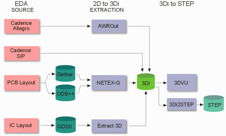
The flow chart below shows how we connect EDA tools to MCAD tools via the STEP format.

Note the modular approach. First one has to extract or export EDA layout data; then the 2 1/2D layered data has to be extruded into 3D. Finally the 3D data is converted into STEP.
While this may appear to be unnecessarily complex, there are good reasons for this modular approach.
supports a wide variety of input formats
enables finer grained control of what gets translated
leverages existing mature EDA translators
We have noticed that there are two distinct targets for the 3D STEP description of a PCB or micro-circuit.
FFF- Form Fit and Function
These users are making 3D models of their boards for purposes of illustration or helping to integrate the board into a package, system or test fixture. These users generally only care about the top and bottom sides of the board: the components, the traces and solder masks, the mounting holes and possible the silk screen. They don't care about inner layer geometry or vias which can represent a very large amount of 3D data. They would like the 3D data to as compact as possible -- this means that if we can describe geometries using arcs instead of segments that the files will be smaller and easier to import and place.
In many cases these users replace the crude rectangular representation of a component or connector with a more detailed one suitable for illustrative purposes. Such 3D models are then useful for all sorts of documentation.
FEA- Finite Element Analysis
These users are making 3D models in order to simulate the electrical, thermal and/or stress properties of their PCB/package. Because the next step is typically to run the data through the meshing process, they have some very strict requirements on the "quality" of the data. All surfaces of butting materials must mate perfectly. No solid bodies may interfere. Arcs are generally not desired. Resolution is kept as low as possible to minimize the number of mesh triangles. Internal modeling of the vias is critical. The ability to select geometries effectively and assign them properties such as net and material is critical.
In order to meet the requirements of this group of users we have had to implement a number of very sophisticated geometric operations. So much so that we have decided to branch our STEP output specifically for FEA/simulation applications.