Generic 300 MM Wafer RDL Layout
Because most data files we deal with are proprietary I decided to create a "generic" RDL layout arrayed on a 300 mm wafer. I wanted a file that was big enough to tax the rasterizer and which has a good mix of repeating data (i.e. cell placements) and non repeating data.
The RDL Circuit
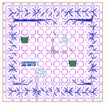
I started by using AutoCAD to create a basic RDL circuit using a circuit size of 5000 x 5000 um. I used a bump pad of diameter 298 um with a pitch of 400 um. For the via connections to the die I created a square opening of 10 x 10 um. I connected the bump pads to the via openings with a trace of 2 um in width. In order to generate more complexity I "poured" a ground plane on the entire RDL layer leaving openings for a few fake interdigitated capacitors and a logo. I also threw in a number of "holes" into the copper pour, again to increase the complexity of the circuit.

Once I was satisfied with my RDL circuit I converted it into GDSII format.
Stepping the RDL Circuit
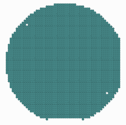
I then used Artwork's GDS-SR step and repeat software to step this RDL circuit across a 300 mm round region with a street width of 185 um. This generated 2394 die inside the margin and 325 die that crossed or touched the margin and would be considered bad die. I knocked out a few die along the bottom and a few in two corners to act as openings for the underlying wafer. (There are usually either test devices or alignment marks where the underlying wafer is exposed.
At this point I have a large number of stepped circuits but no "flat" data.

This file is very small (2 MB) since the only flat data is that contained in the cell definition.
Clipping at the Periphery
Depending on the process, it is usual to "clip" the array at the wafer periphery and to replace the outer 2-3 mm of circuits with a solid ring of metal. This is a two step process - first use a program called Hextract to clip any cells that cross the margin and then drop in a 300 mm diameter "ring" of width 2-3 mm.
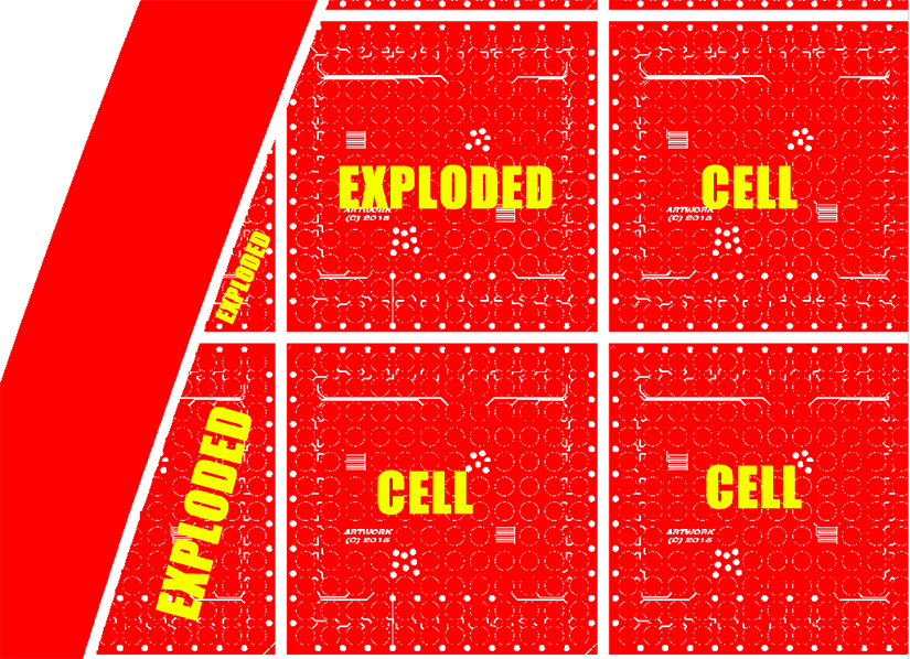
The result of the clipping is that any cell that crosses the margin is exploded and the entities within that cell are clipped. This will generate a very large amount of "flat" data which is exactly what I want. You can see an enlarged view of the left side of the device after these steps.

The size of the GDSII file is now increased to almost 200 MBytes. And this is our sample for testing rasterization, edge bias (sizing) and distortion correction.
While this GDSII File is too big to post, interested and qualified parties can contact Steve DiBartolomeo and I can arrange for you to download it.
Edge Bias Before Raster
Prior to running our raster tests and benchmarks, this file is run through Artwork's SFGEN software. SFGEN re-organizes the data in a way that tells the rasterizer what data is safely repeated and what data must be rasterized completely.
Even more important is edge bias. Since many raster imaging machines have a beam diameter that is quite a bit larger than the address size, the masks produced would have geometries that "leaked" out past the desired edges by about 1/2 of the beam diameter. So prior to raster, SFGEN is used to "shrink" all edges by 1/2 of the beam diameter.
This is why you will note that while I drew the narrow lines as 2 um, when measuring the GDSII for distortion they were only 1 um wide. The missing 1 um is due to the edge bias that was applied by SFGEN.
