

Perhaps the most common use of WMEdit is to convert from one map format to another. In this example we are going to:
a) open a MAP file in the TEL P8 format
b) convert it to the SINF file format
c) map the bin codes used by the TEL P8 into specific Bin codes for the SINF file
Our target machine reads SINF and it expects the following bin codes: 01-PASS, FF-FAIL. The wafer flat should be on the bottom
We start by opening the TEL P8 File. (Remember one must specify the format in the Open File dialog). Here is what it looks like:
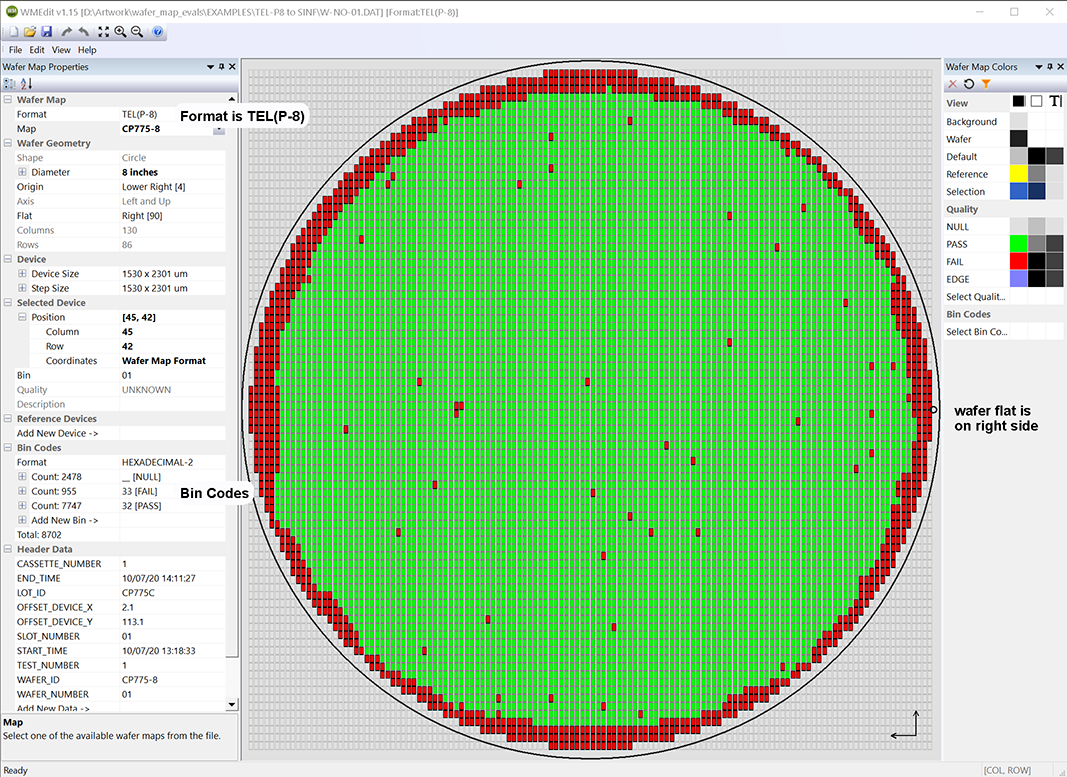
Three Things to Note
a. Notice in the Format field the value is TEL(P-8)
b. Notice that the flat/notch is located on the right side
c. Notice the Bin Codes - 32-PASS and 33-FAIL
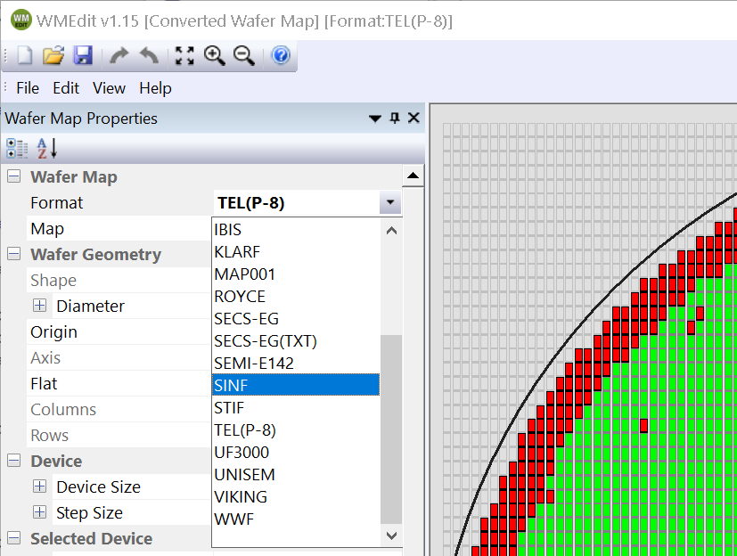
Change the Format to SINF.
You do this by selecting the drop down button next to Wafer Map Properties | Wafer Map Format | Format and selecting the format "SINF".
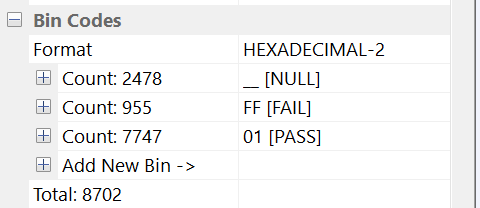
Map the Bin Codes.
Our target machine needs SINF (in HEX) with 01=PASS and FF=FAIL. So we go to the Bin Code section of the Wafer Map Properties Dialog and change 32 to 01 and 33 to FF. The null bin code __ is the same for SINF so no need to modify that.
Rotate The Wafer
Our target machine needs the wafer flat/notch on the bottom - the data from the P8 has the flat/notch on the right. A 90 degree clockwise rotation will present the SINF map to the target machine in the direction it requires.
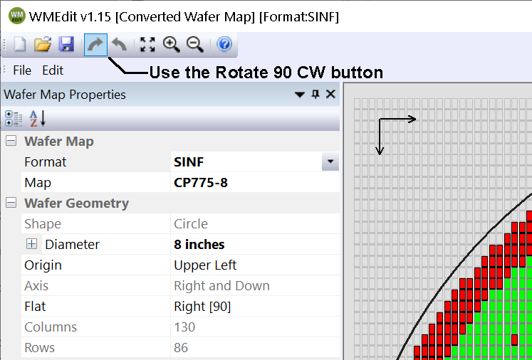
Our WMEdit display now shows the flat/notch on the bottom of the wafer.
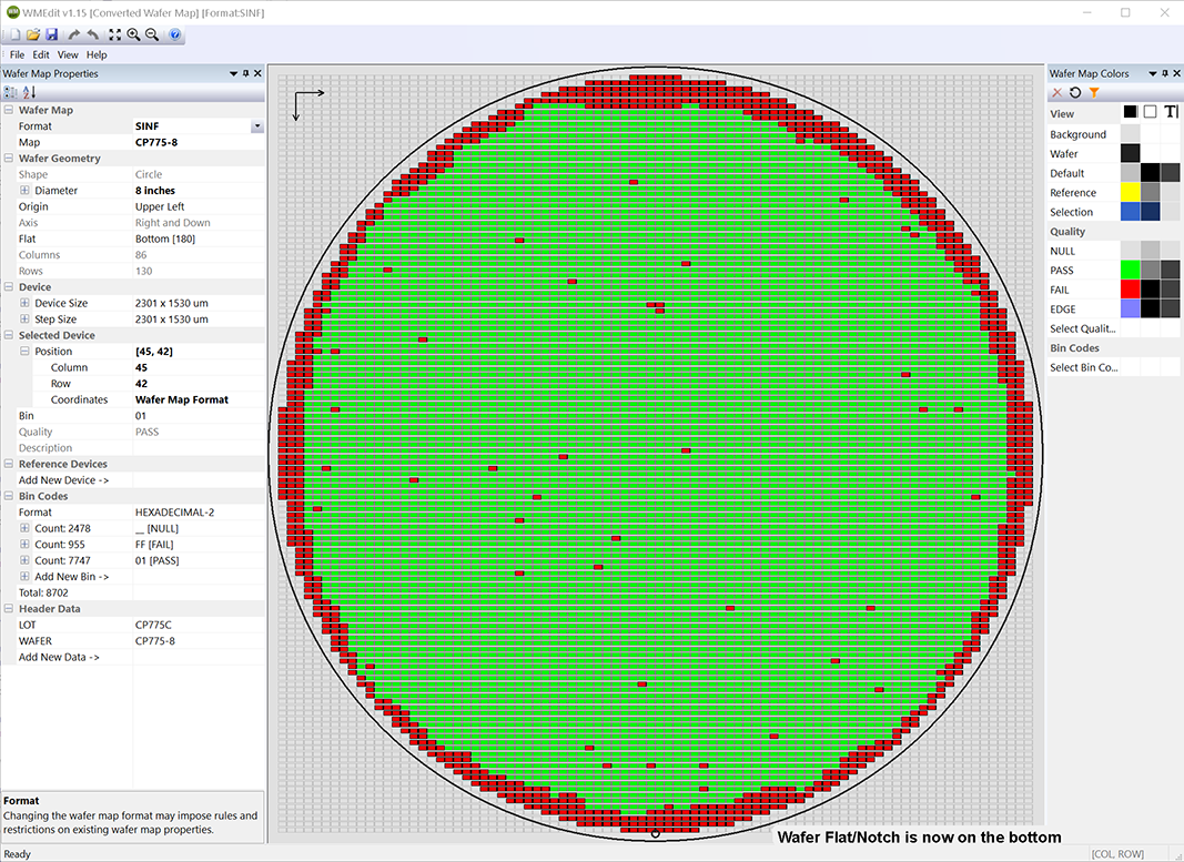
Now that we have set the format to SINF, mapped the bin codes to the desired ones and rotated the wafer to get the flat on the bottom we are ready to save the new map file.
Use the File | Save As menu pick and select the name for your new file.
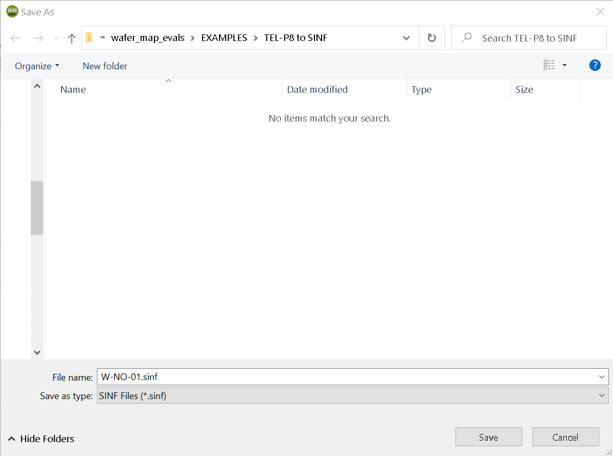
Let's have a quick look at the SINF file to see what it looks like:
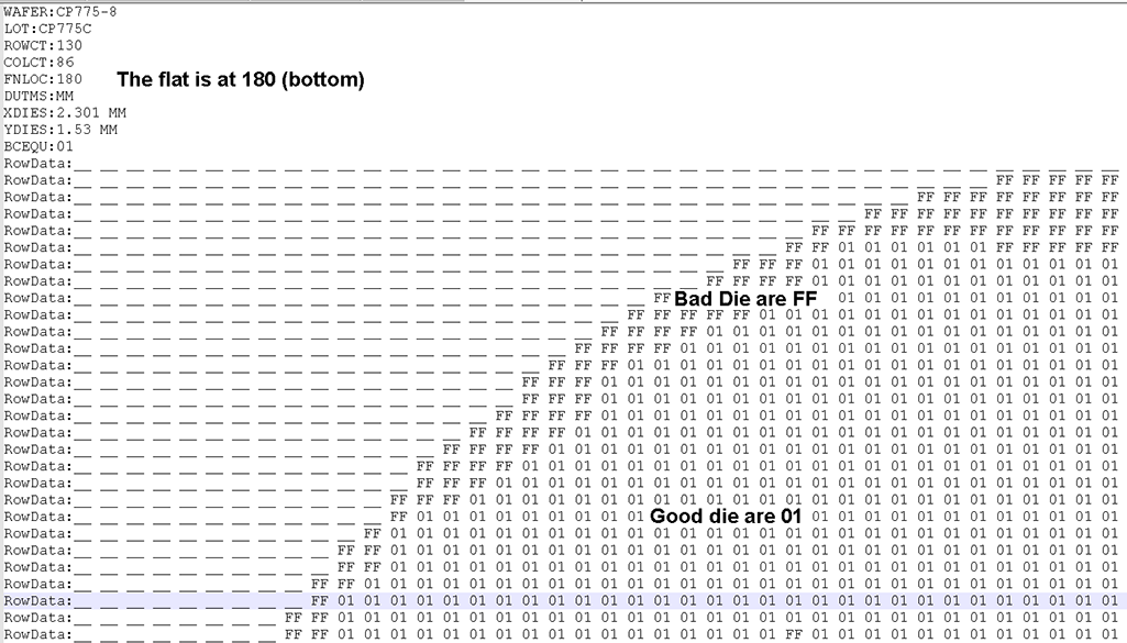
From the header we can see that the FNLOC = 180 which is on the bottom of the wafer.
When we examine the device map we see that the good die = 01 and the failed die = FF.
So we have met the requirement for the target machine.
Back to the Table of Contents