

|
Extracting a Net ListJanuary 10, 2017 Steve DiBartolomeo A client of Artwork needed to extract a net list from a flip chip package design. They already had a net list from the original design (created in APD) but the test lab had requested the manual addition of "jumpers" across many of the die pads and many of the ball pads to create a daisy chain variation. After the addition of the jumpers a new net list had to be extracted to insure that the correct connections had been made. 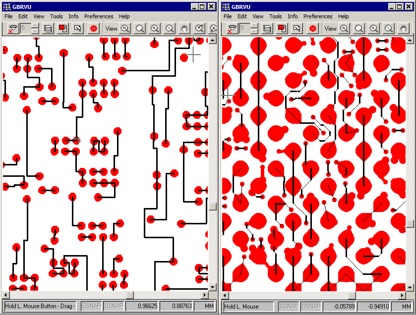 Left side: die.gbr - jumpers added to die side; Right side: rdl.gbr - jumpers added to BGA side. The client was able to use NETEX-G to create a new set of nets based on connectivity taking the jumpers into account. Pin labels were imported using the AIF format - AIF can be exported from the original APD design since the locations of the pins and their labels is not affected by the addition of the jumpers used to produce a daisy chain. Step 1 - Gather the DataTo extract the nets and produce a proper netlist we used: die.gbr - a Gerber file that included the die pads plus the jumpers on the die side via.gbr - a Gerber file that contained the vias from the die pads to the RDL rdl.gbr - a Gerber file that contained the RDL metal plus jumpers added to the RDL side package.aif - an AIF file that contained the die pad locations, labels and coordinates Step 2 - Put Top/Bottom Conductors into NETEX-GStart NETEX-G and load the die.gbr and rdl.gbr files into positions 1 and 3. Insert a dielectric between them. 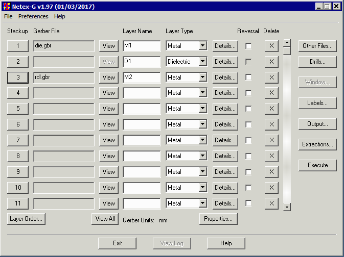 Next we need to connect the die pads to the RDL layer. This is done using the via.gbr file and defining it as a drill between the two layers. Step 3 - Using the Drill Dialog to Connection Top/BottomThe drill dialog defines one or more drills that are used to produce vias between conductor layers. In this case we use the via.gbr layer as our drill (even though this process uses no actual drills we still use this nomenclature from the PCB business.) 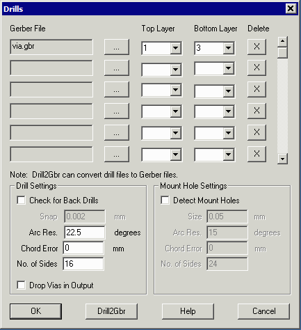 Notice that we set the top and bottom layer to 1 and 3 - this is the stackup position since position 2 is a dielectric between the two conductor layers. Step 4 - Define Vertical PropertiesWhy do we need to define vertical properties for net list extraction? We don't; but because we are using a flow that produces a 3D output file we are required to define Z thicknesses for the conductor and dielectric layers. This is done by cliking on the Properties button from the main dialog and filling in some reasonable values. 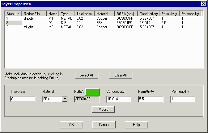 Step 5 Import Labels from AIFNetex-g can trace out connected geometries without any external labels but these results would not be useful. Fortunately we can mass import the locations of the pins (both die side and BGA side) from the AIF file exported from APD. (Note - it is important that when you export AIF and generate your Gerber data that there not be any X,Y offset between them and that they share the same mirroring. Just like a probe card for a PCB must not be mirrored or shifted.) We import the pin information using the Labels dialog box; then select Import and AIF. 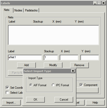 Use the browse button to select your AIF file and then check: Import Nodes from AIF. (Nodes are the NETEX-G equivalent to pins) Select Ball Pads and Die Pads. Turn on: Use Ref Des and enter the appropriate reference designator. Make sure you have the stackup layer correctly selected. In this example we put the die pads on 1 and the BGA on 3 but we could have loaded in the other order. 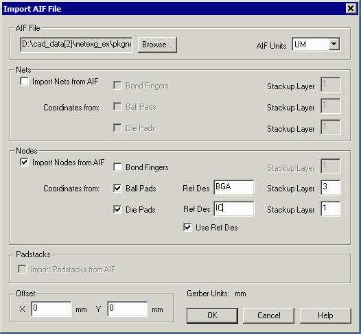 Then click on OK. When you get back to the Label dialog box you will see that the Nodes section now has data. You should see all the pin labels imported from the AIF as shown below: 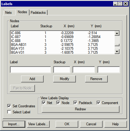
Step 6 - Define the OutputWe get to the output dialog by clicking on the Output button from the main menu. Once in this dialog we make the following settings: 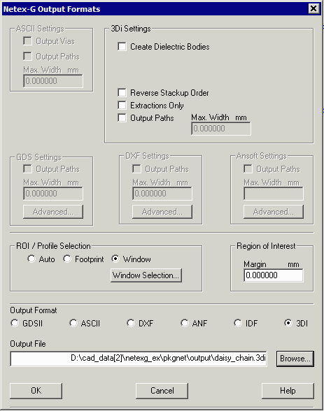 We set our output format to: 3Di. We don't need to check: Create Dielectric Bodies since we are just considering the conductors. The ROI/Profilie section should be set to Window. Then click on the Window Selection Button and make sure the window is set to Data Extents. 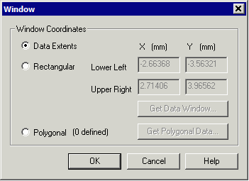 Finally we define an output file name for our 3Di file. This will normally be placed in the directory we defined for output in the preferences dialog. That's it for the output dialog. Step 7 - Running the ConversionFrom the main menu, click on the Execute button. The program will prompt you to save the job file (an ascii file that contains all your settings and which can be reloaded in future sessions) Then it will process the Gerber files and the pin label data. When NETEX-G is complete, there should be two files in the output directory:  The 3Di file can be viewed using Artwork's 3DVU and it displays a geometric representation of the layout. 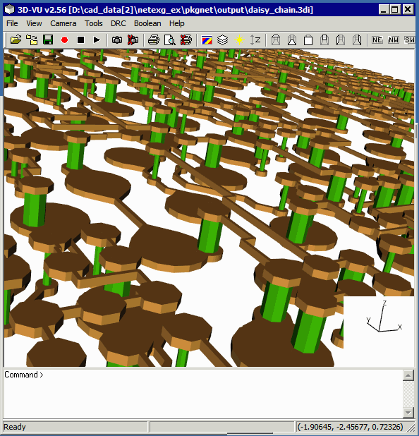 The text file is a netlist sorted by Net with one reference designator/pin per line along with its X,Y coordinates. (the X,Y coordinate are always converted into units of microns even through the Gerber data is in inches or mm.) 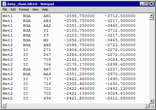 This netlist is always created when 3Di output is created. However, if no pin labels were imported or defined, then the netlist file will be empty. |