Specific Issues when Writing ANF
Ansoft's Neutral File
Polygon Geometry
ANF polygons should be created using the Leonov polygon option. This option is selected in the Preference's Dialog.

Polygons Only
Netex-G flattens and booleanizes all of the Gerber data into polygons. This means you cannot get traces (also
called C-lines) into ANF format. The only C-lines going to ANF are wires.
Dielectrics
There must be a dielectric between metal layers. If no such layer is present in the NETEX-G stackup,
the ANF reader will insert a dielectric layer. This is not good as it then changes the stackup positions and
things such as vias will be messed up. No dielectric is needed (or desired) between wire layers and metal layers.
Wires
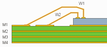
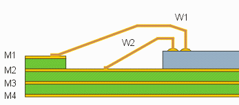
A wire layer must appear immediately above the metal layer that it connects to. For most BGA's this is not complicated but if your package has several shelves of fingers then you must make sure the stackup is correct or your wires won't be attached to the package.

The stackup for this type of geometry would look like:
Stackup     Layer   Layer
Position    Name    Type

   1         W1     WIRE
   2         W2     WIRE
   3         M1     METAL
   4         D12    DIELECTRIC
   5         M2     METAL
   6         D23    DIELECTRIC
   7         M3     METAL
   8         D34    DIELECTRIC
   9         M4     METAL

This design differs in that the wires don't all land on the same layer of metal. Hence it is important when defining the stackup to make sure that each wire layer immeidately precedes the metal layer that it is attached to.
Stackup     Layer   Layer
Position    Name    Type

   1         W1     WIRE
   2         M1     METAL
   3         D12    DIELECTRIC
   4         W2     WIRE
   5         M2     METAL
   6         D23    DIELECTRIC
   7         M3     METAL
   8         D34    DIELECTRIC
   9         M4     METAL
ANF based tools assume that one end of the wire connects to the package and the other end (the free end) connects to the die. The "port" for analysis starts at the free end of the wire. Hence you do not need any die pad data or layer.
NETEX-G will automatically create a "pseudo" via from the outer end of the wire to the metal layer below it.
This via has no height, is round and is the same diameter as as the wire. ANF products detect this via and
that is how they determine which end of the wire is connected to the package and which end is "free"
Solder Ball Pads
Most ANF based tools require a pad in order to attach a solder ball to the pad. In a typical BGA, this might be the ball
pad. The easiest way to generate such a pad is to use a Gerber file that contains the ball pads and treat it as a "drill"
file that goes through only the bottom layer.
Another way to generate the required pad is to use the node label and make sure to associate that node with a user defined padstack. This method is most effective when you have an AIF file from the package design that contains the ball pad coordinates.
|

