Creating Hybrid Circuit Artwork Using AutoCAD and ASM 500
by Steve DiBartolomeo
Introduction
This note explains how to draw hybrid circuit artwork using AutoCAD. Since AutoCAD does not drive the photoplotter used to produce film, the AutoCAD DXF file must be run through a translator. The designer that understands the hybrid fabrication process and photoplotting techniques will get correct results with a minimum amount of effort and expense.

High Resolution Needed
Narrow lines and gaps are the most critical part of the hybrid to etch. Hybrids for microwave applications include coupler fingers less than 1 mil wide with gaps of 0.9 mil.
Very few photoplotters can directly image 1 mil lines and gaps so often a 10X plot is made and reduced on a process camera. At 10X an entire 2X2 inch snapstrate can be plotted on a single piece of 20 X 20 inch film.
Masks Required
Two separate photomasks are required: one to pattern the metal layer and a second for the resistor layer. Masks are chrome on glass. The glass mask is produced by reducing 10X photoplot on a precision camera.
AutoCAD Layering System
The following layer are created on AutoCAD to draw the hybrid. Several of these layers are not imaged but contain data necessary for the blue print and documentation. ASM 500, the DXF to Gerber translator, selects data from a specified layer and ignores data on other layers when creating Gerber data.
|
| METAL |
 |
Defines metal areas to be filled on mask. Many hybrids have two or more layers of metal. There may also be layers defined for inner polygons.
|
| RESISTOR |
 |
Defines resistor patterns for mask. Some hybrids, especially thick film processes, might have three, four or even five different resistor layers and associated masks. |
| OUTLINE |
 |
Outline of circuit. This layer is normally not plotted but is useful
when setting up your step and repeat. |
| FIDUCIAL |
 |
Fiducials. This layer is optional. Generally one would like a border around
the entire mask with alignment marks and text. |
| TITLE |
 |
Title Border. This layer is not photplotted but is used for
blue prints and assembly or process documentation. |
Setting up Auto CAD Layer and Parameters
|
Create the basic layers:
METAL
RESISTOR
OUTLINE
FIDICUIAL
TITLE
|
Additional layers for documentation or advanced processing, such as polymide via layers, backside metal, or multiple resistor layers, may be present.
|
Set the AutoCAD drawing limits to 0,0 and 3,3 if you are working in inches. Set 0,0 and 3000, 3000 if you are working in mils.
Set SNAP on. This is very important to insure that line endpoints touch exactly. A grid snap of 0.001 in. is reasonable.
Drawing the Outline
 |
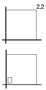
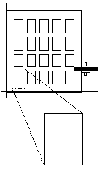
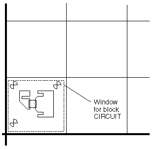
Set the current layer to OUTLINE. Draw a 2 x 2 inch square which defines the area of the snapstrate. In the lower left hand corner of the 2 x 2 outline draw another box that represents your circuit size. For example, the individual circuit may be 0.25 x 0.4 inches. Using the ARRAY command, array the outline of the circuit to fit inside the 2 x 2 inch box. Account for any clearance required from the edge of the snapstrate as well as the between parts to allow the cutting saw kerf. |
|
When finished calculating the correct outline size and clearance you will have a drawing similar to the one at right. Zoom in on the circuit outline in the lower left corner. Draw your single circuit inside this area; when complete make it into a block, and then array the block using the outline as a guide.
|

|
Drawing the Metallization
Set the current layer to METAL. Begin drawing the figures that will be metal areas on the mask. Define each figure using a zero width closed polyline. If you are interconnecting pads with circuit traces you can also use a polyline with width for the interconnects. Each boundary will be filled solid during translation. Use grid snap or object snap to insure that all the line endpoints are exactly touching.

Properly drawn figures in AutoCAD (at left)
will be filled in by the ASM 500 translator and appear on the film at right.
|
Drawing Errors to Avoid
- Extraneous lines that touch the boundaries. These are detected by the post processor and may affect your photoplot. These are extremely hard to see if they are covered by another larger line.
- Figures insides of figures: The larger outer figure will cover up the inner figure
- Boundaries that self intersect
|

|
[A] Figure self intersects. The filling routines will not work correctly.
|
[B] Endpoints don't meet. Figure is not filled by processor. The effect is exaggerated in this example. In may cases, the overlap is not easily visible in AutoCAD.
|
[C] Designer intended the inner polygon to be empty on the film. However,the outer polygon covered it. Put the inner polygon on s different layer or draw around it.
|
Drawing the Resistor Layer
Set the current layer to RESISTOR. Using layer METAL as your reference, draw the resistors. Most resistors are rectangles. You can use a zero width polyline to define each rectangle. It is also possible to use lines, solids, or polylines with width. ASM 500 will recognize any of the above forms and fill in the rectangles on the film.
|

|
|
|
The resistor boundary can be from lines or zero width polylines [A] or from plines with width [B].
|
Drawing "Islands and "Holes"
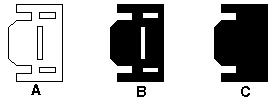
Islands and holes are areas of clear film surrounded by dark film, or after the processing, areas of no metallization surrounded by metallization. A very common mistake is to simply draw the island area as a figure surrounded by the metallized area. This is not going to work as the outer area will cover the hole.

The designer drew the figure [A] expecting to get figure [B]. Instead, the film came back as in figure [C]. The mistake was that the inner polygons were covered while filling the outer polygon. One should create a separate layer for the inner polygons and have the photoplotter do a composite plot.
There are several drawing strategies that avoid covering the holes. The most powerful technique is to use the ability of laser photoplotters to do composite plotting. A laser photoplotter can read several Gerber files and plot them on a single sheet of film. The data on any layer can be added or subtracted from data on another layer.
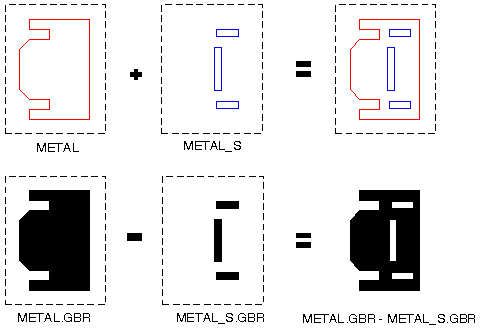
The subtractive process is used for plotting islands. The procedure is simple. Create one or more additional AutoCAD layers to hold the inner polygons. Then draw the inner polygons or "holes" on the layer assigned to this purpose. Produce two Gerber files: one for the outer polygons and a separate one for the inner polygons. Then tell the photoplot operator to subtract the hole layer.
Example -- Create the basic AutoCAD layers adding one for inner polygons:
METAL
METAL_S
RESISTOR
OUTLINE
FIDICUIAL
TITLE
After drawing the outer metal figures on layer METAL, set the current later to METAL_S. Now draw the inner polygons on layer METAL_S. You will produce two Gerber files; one from layer METAL and one from METAL_S. When METAL and METAL_S are plotted, be sure to indicate that they should be merged; have METAL_S subtracted from METAL.

By creating seperate AutoCAD layers for the inner polygons, a composite plot will create complex groundplanes with islands and holes.
|
Arraying the Data
Whether you should array your circuit depends on it's complexity. If the circuit is simple then send the photoplotter arrayed data. Complex circuits produce files too large to transfer easily to diskettes or by modem.
To array the data on AutoCAD use the BLOCK command. Turn on the metal, resistor, and outline layer. Define a block called circuit at 0,0. Do not scale or rotate the block. Using the AutoCAD array command, and the array data you calculated when creating the outline layer, array the block circuit.
|

|
Once the basic circuit is complete, make it into a block. Insert and array the block.
This minimizes the size of the AutoCAD file and speeds the translation to Gerber. However, it does not reduce the eventual size of the Gerber file.
|
|
Before arraying the circuit, save the drawing file under a different name. You will have a drawing file of the single circuit in case changes need to be made. It is easier to modify the file and array again, rather than edit the arrayed file.
After you've finished the array and checked it, create a DXF file. Use the default six places of data. If your drawing contains unused layers and blocks, erase these layers/blocks and purge the drawing file to eliminate the extraneous data. While this is not mandatory for the post processor, it wills reduce the translation time required.
Configuring ASM 500
Before running the translator you need to configure it properly. This will depend on the type
of photoplotter you are using. Photoplotter's can be broken down into 3 basic types:
- 1. Those that support RS274X.
- 2. Those that support MDA (FIRE 9000 family)
- 3. Those that require stroked fill data (vector and other laser plotters).
|
FORMAT 4.4
SUPPRESS LEADING
SUPPRESS CR
FONT C:\ACAD\SOURCE\TXT.SHP
D10 0.002 D
D11 0.004 D
D12 0.008 D
D13 0.015 D
D14 0.025 D
D15 0.040 D
|
- Sets Gerber format to 4 integar and 4 decimal places.
- Suppresses leading zeros in Gerber file.
- Text will be plotted using AutoCAD's TXT.SHP font.
- Apertures for filling start at 0.002 inch and double up to 0.040 inch.
The post processor will chose a small aperture around the edge of each figure
and use larger apertures to fill the interior.
|
Running the Post Processor
Make a list of the layer to plot and the units of the drawing. Start up the ASM500 program and answer the menu items appropriately. When completed, the program will have produced one Gerber file for each AutoCAD layer that was selected for processing.
|
In this example one would have:
| AutoCAD Layers |
Gerber Photoplot Files |
| METAL |
METAL.GBR |
| METAL_S |
METAL_S.GBR |
| RESISTOR |
RESISTOR.GBR |
| FIDUCIAL |
FIDUCIAL.GBR |
Sending Data and Instructions to the Photoplot Shop
The Gerber files can be sent by modem or floppy diskette to the photoplot shop. Note that
the Gerber files alone are not sufficient to plot a film. You must accompany the files with information on the actual apertures used and diameters. You should also indicate how you want each file plotted.
Plot Instructions for project: HYBRID
Image size is 20 x 20 inches; data is absolute format 4.4 leading zeros supressed.
FILM1 Metal Pattern (merge to the following files) Plot positive.
FUDICIAL.GBR     PAINT
METAL.GBR        PAINT
METAL_S.GBR      SCRATCH
FILM 2 Resistor Pattern (merge the following files) Plot Positive
FIDUCIAL.GBR     PAINT
RESISTOR.GBR     PAINT
APERTURE LIST
D10             0.002 ROUND
D11             0.004 ROUND
D12             0.008 ROUND
D13             0.015 ROUND
D14             0.025 ROUND
D15             0.040 ROUND
Please produce 4 inch chrome masks by 10:1 photoreduction. Masks should be RRED,
dark field. Dark field should extend to the edge of the glass.
|

|
Display of the AutoCAD hybrid drawing. The rectangular cutouts are solder dams. They are drawn on METAL_S and subtracted from the data on layer METAL. The resistors were drawn with the polylines of the appropriate width.
|

|
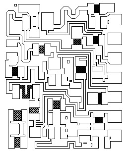
Photoplot of the metal mask. The AutoCAD DXF file and associated Gerber plot files can be obtained on floppy diskette by contacting us.
|
